AMO – Neue Wege für Innovationen
Exzellente Forschung aus Aachen
AMO GmbH ist ein gemeinnütziges Forschungsunternehmen auf dem Fachgebiet der Nanotechnologie. Seit über 30 Jahren agiert AMO als Wegbereiter für neue Technologien an der Schnittstelle zwischen akademischer und industrieller Forschung. Kernkompetenzen sind Graphenelektronik, Nanophotonik, Nanostrukturierung, Sensorik und Perowskit-Optoelektronik. AMO ist ein weltweit gefragter Partner von Innovator*innen, die neue und unkonventionelle Wege gehen wollen und die neuesten Erkenntnisse der Forschung in neue Anwendungen umsetzen.

Aktuelles
Unsere News
 https://www.amo.de/wp-content/uploads/2024/04/NRW-delegation-Piedmont.jpg
236
627
Dr. Federica Haupt
https://www.amo.de/wp-content/uploads/2021/03/AMO_Logo.jpg
Dr. Federica Haupt2024-04-16 18:17:192024-04-16 18:22:25Institutioneller Besuch in Piemont
https://www.amo.de/wp-content/uploads/2024/04/NRW-delegation-Piedmont.jpg
236
627
Dr. Federica Haupt
https://www.amo.de/wp-content/uploads/2021/03/AMO_Logo.jpg
Dr. Federica Haupt2024-04-16 18:17:192024-04-16 18:22:25Institutioneller Besuch in Piemont https://www.amo.de/wp-content/uploads/2024/04/flexible-CMOS-Inverter-pssa-Piacentini.jpg
264
365
Dr. Federica Haupt
https://www.amo.de/wp-content/uploads/2021/03/AMO_Logo.jpg
Dr. Federica Haupt2024-04-12 12:22:112024-04-12 12:33:59Erste Demonstration eines CMOS-Inverters auf Basis von TMDC auf einem flexiblen Substrat
https://www.amo.de/wp-content/uploads/2024/04/flexible-CMOS-Inverter-pssa-Piacentini.jpg
264
365
Dr. Federica Haupt
https://www.amo.de/wp-content/uploads/2021/03/AMO_Logo.jpg
Dr. Federica Haupt2024-04-12 12:22:112024-04-12 12:33:59Erste Demonstration eines CMOS-Inverters auf Basis von TMDC auf einem flexiblen Substrat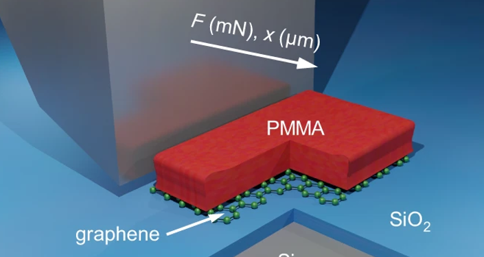 https://www.amo.de/wp-content/uploads/2024/03/ButtonShearTest.png
475
705
Dr. Federica Haupt
https://www.amo.de/wp-content/uploads/2021/03/AMO_Logo.jpg
Dr. Federica Haupt2024-03-21 09:22:462024-03-21 09:39:16Neue Veröffentlichung in Nature Communications zur Messung der Adhäsion von 2D-Materialien
https://www.amo.de/wp-content/uploads/2024/03/ButtonShearTest.png
475
705
Dr. Federica Haupt
https://www.amo.de/wp-content/uploads/2021/03/AMO_Logo.jpg
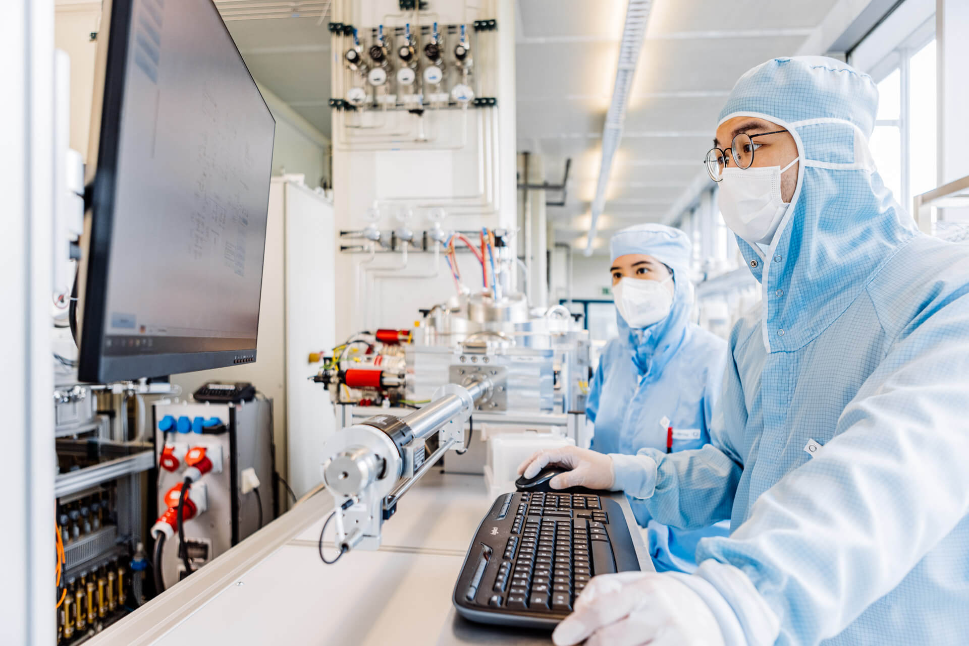
Dr. Federica Haupt2024-03-21 09:22:462024-03-21 09:39:16Neue Veröffentlichung in Nature Communications zur Messung der Adhäsion von 2D-Materialien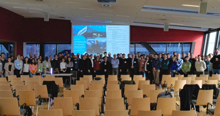 https://www.amo.de/wp-content/uploads/2024/02/P1056763-E-scaled.jpg
1278
2560
Dr. Federica Haupt
https://www.amo.de/wp-content/uploads/2021/03/AMO_Logo.jpg
Dr. Federica Haupt2024-02-29 10:33:062024-02-29 13:10:31Zwei inspirierende Tage zum Thema 2D-Materialien
https://www.amo.de/wp-content/uploads/2024/02/P1056763-E-scaled.jpg
1278
2560
Dr. Federica Haupt
https://www.amo.de/wp-content/uploads/2021/03/AMO_Logo.jpg
Dr. Federica Haupt2024-02-29 10:33:062024-02-29 13:10:31Zwei inspirierende Tage zum Thema 2D-MaterialienTestimonials
Was unsere Partner sagen
Offene Stellen
Die nächste Generation an Expert*innen
Bei AMO verstehen wir Forschung nicht nur als Mittel zur Gewinnung neuer Erkenntnisse, sondern auch zur Ausbildung der nächsten Generation von Wissenschaftler*innen und Techniker*innen. Informieren Sie sich über unsere offenen Stellen.


![]()